(China (Mainland))

Product Summary
These devices are precision timing circuits capable of producing accurate time delays or oscillation. In thetime-delay or monostable mode of operation, the timed interval is controlled by a single external resistor andcapacitor network. In the astable mode of operation, the frequency and duty cycle can be controlledindependently with two external resistors and a single external capacitor.
The threshold and trigger levels normally are two-thirds and one-third, respectively, of VCC. These levels can bealtered by use of the control-voltage terminal. When the trigger input falls below the trigger level, the flip-flop isset, and the output goes high. If the trigger input is above the trigger level and the threshold input is above thethreshold level, the flip-flop is reset and the output is low. The reset (RESET) input can override all other inputsand can be used to initiate a new timing cycle. When RESET goes low, the flip-flop is reset, and the output goeslow. When the output is low, a low-impedance path is provided between discharge (DISCH) and ground.The output circuit is capable of sinking or sourcing current up to 200 mA. Operation is specified for supplies of5 V to 15 V. With a 5-V supply, output levels are compatible with TTL inputs
Parametrics
Absolute Maximum Ratings(1):
over operating free-air temperature range (unless otherwise noted)
(1)VCC,Supply voltage(Note2):18V;
(2)VI,Input voltageCONT, RESET, THRES, TRIG:VCC V;
(3)IO,Output current:±225mA;
(4)θJA,Package thermal impedance(Note3)(note4):85℃/W;
(5)TJ,Operating virtual junction temperature:150℃;
(6)Tstg,Storage temperature range:-65℃ to 150℃
Note:
(1)Stresses beyond those listed under "absolute maximum ratings" may cause permanent damage to the device. These are stress ratingsonly, and functional operation of the device at these or any other conditions beyond those indicated under "recommended operatingconditions" is not implied. Exposure to absolute-maximum-rated conditions for extended periods may affect device reliability.
(2)All voltage values are with respect to GND.
(3)Maximum power dissipation is a function of TJ(max), θJA, and TA. The maximum allowable power dissipation at any allowable ambienttemperature is PD = (TJ(max) - TA)/θJA. Operating at the absolute maximum TJ of 150℃ can affect reliability.
(4)The package thermal impedance is calculated in accordance with JESD 51-7
Features
(1)Timing From Microseconds to Hours;
(2)Adjustable Duty Cycle;
(3)Astable or Monostable Operation;
(4)TTL-Compatible Output Can Sink or Sourceup to 200 mA
Diagrams
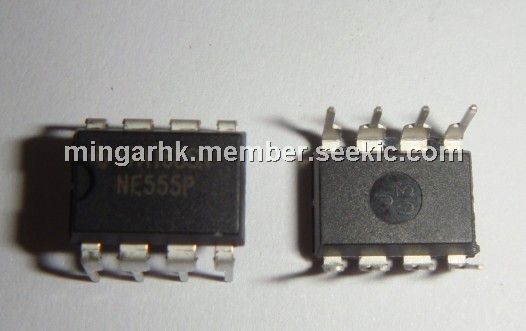
<IMG border=0 src="http://www.seekic.com/uploadfile/ic-mfg/20128162044986.jpg">
| Image | Part No | Mfg | Description |  |
Pricing (USD) |
Quantity | ||||||||||||
|---|---|---|---|---|---|---|---|---|---|---|---|---|---|---|---|---|---|---|
 |
 NE555P |
Texas Instruments |
Timers & Support Products Precision |
Data Sheet |
|
|
||||||||||||
|
NE555PE4 |
Texas Instruments |
Timers & Support Products Precision |
Data Sheet |
|
|
||||||||||||
|
NE555PSRE4 |
Texas Instruments |
Timers & Support Products Precision |
Data Sheet |
|
|
||||||||||||
|
NE555PSR |
Texas Instruments |
Timers & Support Products Precision |
Data Sheet |
|
|
||||||||||||
|
NE555PW |
Texas Instruments |
Timers & Support Products Sgl Prec Timer |
Data Sheet |
|
|
||||||||||||
|
NE555PSRG4 |
Texas Instruments |
Timers & Support Products Sgl Prec Timer |
Data Sheet |
|
|
||||||||||||
|
NE555PWE4 |
Texas Instruments |
Timers & Support Products Sgl Prec Timer |
Data Sheet |
|
|
||||||||||||
|
NE555PWG4 |
Texas Instruments |
Timers & Support Products Sgl Prec Timer |
Data Sheet |
|
|
||||||||||||